Thin Film Ceramic Substrates

Quality Beo Ceramic Materials Si3n4 Ceramic Manufacturer Ceramic Materials Ceramics Advanced Ceramics
Thin Film Metallized Substrates Products Maruwa Co Ltd

Thin Film Substrates For Microelectronics Coorstek Technical Ceramics
Thin Film Substrates Fine Ceramics Advanced Ceramics Kyocera
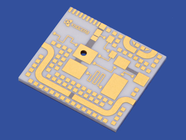
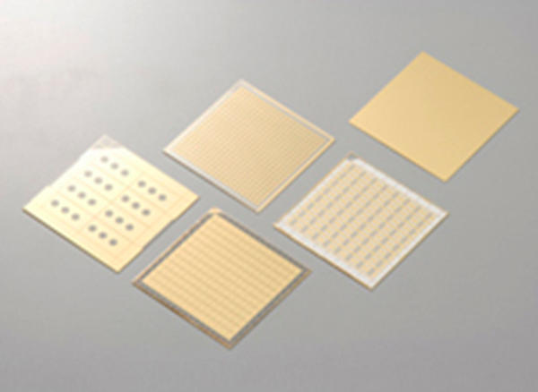
Thin Film Mic Substrates Components For Wireless Communication Devices Ceramic Packages Products Kyocera

Tape Casting Of High Dielectric Ceramic Substrates Google Search It Cast Substrate Tape

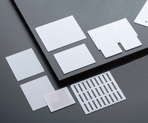
Thin film substrates made of 99 6 alumina offer superior surface smoothness.
Thin film ceramic substrates. Request technical information or a quotation for. Thick copper thin film circuits for high performance applications. Coorstek controls surface finish grain size and surface imperfections to enhance fine line resolution spacing and yields in your thin film process. Mpt thick film technology is robust economical and can reduce the footprint of your circuit.
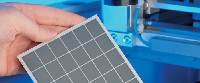
Our precision etching technology pushes thick film ceramic substrates to a best in class position offering the tightest tolerances and the highest performances rivaling thin film capabilities. Multilayer circuits on ceramic with polyimide as the insulator material. If it s possible in thin film chances are it can be realized in etched thick film at a fraction of the price. Why ceramic thin film substrates.
Ceramic substrate requirements. Thin film substrates thin film substrates with superior surface smoothness. Tecdia s engineers push the limits of ceramic technology while maintaining the standard of quality that tecdia has always been known for. The ceramic is screened with conductor insulator and resistor material to form the circuitry.
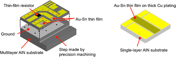
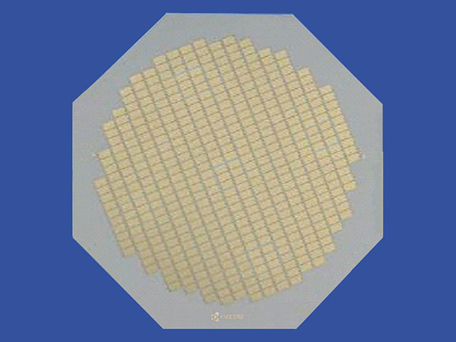
Hybrid circuit ceramic substrates. Therefore high demands with respect to the surface and grainsstructure of the ceramic substrate are made. Thin film ceramic substrates 99 6 alumina up to 300mm diameter and 12 square. Using a wide array of ceramic substrate materials and metal systems combined with advanced thin film manufacturing features and capabilities the circuit designer can now easily reduce circuit size and parts count over traditional thin film substrate design approaches while also enhancing performance.
Thin film substrates on polymer ceramic steel glass ferrite etc. The ceramic powder for the particular sensor substrate material must therefore have a particle size of about 1 micron. Mpt is a one stop shop for your thick film substrate needs. Remtec uses pctf and other advanced technologies to design and produce cost effective custom and semi custom packaging solutions metallized substrates packages and components for power electronics optoelectronics and rf mw applications in commercial industrial and military industries.
The circuits are mainly done for thin film substrates are coated by a pvd process. Thick film substrates are electronic circuit boards generally made from ceramics. Our thin film substrates divisions combine over 35 years of experience in ceramics machining wafer processing and micro circuits into one group that specializes in advanced ceramic substrate technologies. Alumina is an optimal material for most thin film ceramic substrate applications.

Quality Beo Ceramic Materials Si3n4 Ceramic Manufacturer Ceramic Materials Structural Analysis Material Specification

Pin By Ferrotec Nord On Ferrotec Nord Thin Film Film To Focus
Ceramic Substrates Electronic Circuit Carriers And Circuit Boards Made From Advanced Ceramics

Dpc Substrate Thin Film Supply Better Thermal Management And Smaller Dpc Substrate

Sputtering Process Physical Vapor Deposition Vapor Technology

How To Fabricate A Thin Film Composite Membranes By Electrospinning Nanofibers Technology In 2020 Innovation Centre Membrane Material

Pin On Innovacera Ceramic News
Thick Film Substrates Fine Ceramics Advanced Ceramics Kyocera

Nanodiamond Coating Nanodiamond For Electronics Chemical Vapor Deposition Vapor Chemical
Submounts And Subcarriers Components For Fiber Optic Communication Modules Ceramic Packages Products Kyocera
Ceramic Substrates For Probe Cards Ceramic Packages Products Kyocera

Basic Electronics On The Go 14 Fixed Resistors Thick Film And Thin Resistors Basic Electronics

Pin On Crystal Substrates

Quality Beo Ceramic Materials Si3n4 Ceramic Manufacturer Ceramic Materials Advanced Ceramics Properties Of Materials

Aln Crystal Semiconductor Semiconductor Materials Crystal Growth

Thin Film Components And Integration The Next Step In Volumetric Efficiency Inductors Integrity New Product Introduction

Ceramic Substrate An Overview Sciencedirect Topics

Boron Nitride Substrate Heater For Vacuum Deposition Chemical Vapor Deposition Thin Film Ceiling Lights

Quality Beo Ceramic Materials Si3n4 Ceramic Manufacturer Ceramic Materials Advanced Ceramics Properties Of Materials

Thin Film Components And Integration The Next Step In Volumetric Efficiency Disruptive Technology Inductors Integrity

Lead Sulfid Crystal Substrates In 2020 Substrate Crystals Molar Mass

Quality Beo Ceramic Materials Si3n4 Ceramic Manufacturer Ceramic Materials Advanced Ceramics Ceramics

Photo Gallery Furnace Home Decor Copper Foil

Get The Reliable Quality Of Inconel Substrate Heater For Reactive Deposition By The Best Company Substrate Good Things Heater

Zyp Boron Nitride Mold Release Spray Mold Release Ceramic Molds Mold Remover

Classification Of Integrated Circuits Eeeguide Com Circuit Integrity Classification

Pin On Desert Eagle 12 Gauge Related Etc

Quality Beo Ceramic Materials Si3n4 Ceramic Manufacturer Ceramic Materials Advanced Ceramics Ceramics

Innovacera Hot Press Boron Nitride Tube Bn0161150 Inert Gas Melting Metal Thermal Expansion

Pin On Mdc Vacuum Products Division
Ion Beam Sputtering Beams Physical Vapor Deposition Advantage

Analytical Solutions To The Problem Of The Grain Groove Profile Thin Film Online Publishing Solutions

The Film Substrate Material Available From Greenearth Chemicals Includes Laal03 Lasra104 Magnesium Oxide And Ndga03 Fi Thermal Spray Thermal Spraying Spray

Ceramics Week Api S Ceramic Capabilities Capacitors Ceramics Made In America

No Matter What Industry You Re In We Have What You Need To Create A Vacuum Environment And Transfer Energy Light Gas And F Gas Delivery Vacuums Vacuum Pump

Resistor Types Of Resistors Fixed Variable Linear Non Linear Resistors Electronics Basics Diy Electronics

Sputtering Targets At Http Www Greenearthchem Com Product Category Sputtering Targets Ceramics Paneling Display


Boron Nitride Substrate Heater For Vacuum Deposition Chemical Vapor Deposition Thin Film Ceiling Lights

Ox0023 Tantalum Oxide Tantalum Pentoxide Ta2o5 Capacitors Energy Storage Niobium

Manufacturing Image By Rutsoc Chemical Vapor Deposition Gas Delivery Nanotechnology

Sputtering Targets Used In Rf Sputtering Home Stanford Advanced Materials

Silicon Carbide Ceramic Materials Silicon Carbide Ceramics

